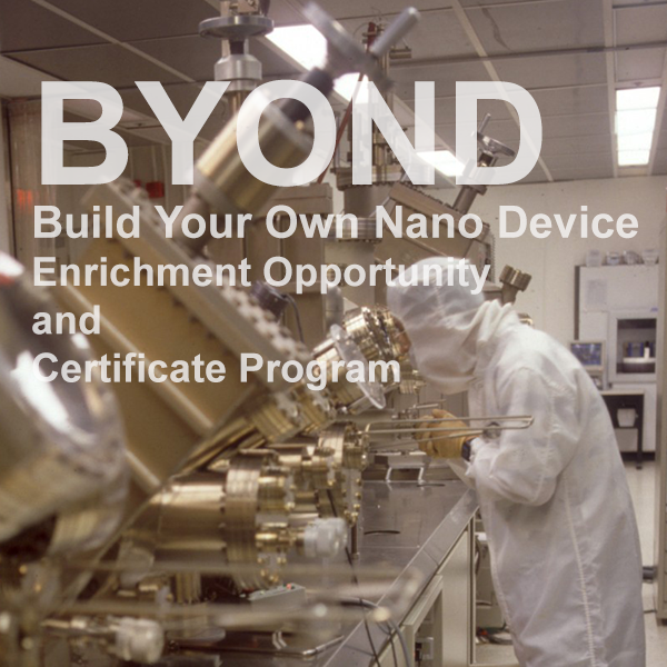
BYOND: Build Your Own Nano Device - Enrichment Opportunity and Certificate Program
The Micro and Nanofabrication Clean Room (MNCR) facility within the Center for Materials, Devices and Integrated Systems (CMDIS) is a Class-100 facility located on the 4th Floor of the Center for Industrial Innovation (CII) building. The MNCR offers a wide range of processing, measurement, and fabrication tools for microelectronics, optoelectronics, MEMS, and other small-scale devices. It has equipment that enables the deposition and etching of thin films, patterning of devices and nanostructures, wet chemical processing, and metrology capabilities.
The growing semiconductor and electronic devices industries and pharmaceutical, medical, optical, solar, and aerospace industries depend on cleanroom technologies where the contamination is controlled. With the increasing demand for engineers and scientists with focused training in cleanroom operations, we offer a certificate program for undergraduate students to start building a foundation. This certificate program is an exciting opportunity for undergraduates, both those planning to pursue a graduate degree and those looking to prepare for a professional career.
This certificate program is designed to introduce microfabrication and analysis concepts to interested undergraduate students. The program currently offers four modules, each running over four weeks. Each weekly lab session will last approximately two hours and consist of classroom instruction and a hands-on laboratory demonstration. A student may take any offered module in any order and is expected to attend each of the four weekly lab sessions. By completing all four modules, the student will be awarded a Microelectronics concentration certificate and be allowed access to cleanroom lab space.
Program and Modules
Module 1 - Lithography (Spin Coating, Optical Lithography, Maskless Lithography, E-Beam Lithography)
Module 2 - Deposition (Vacuum Science, Chemical Vapor Deposition, Physical Vapor Deposition, Atomic Later Deposition)
Module 3 - Metrology (Optical Microscopy, Contact Techniques, Non-contact Techniques, Scanning Electron Microscope)
Module 4 - Etching (Wet Etch, Plasma Physics, Reactive Ion Etching, Gas Deliver and Abatement)
Spring 2025 Modules
Module 4 (Etching) 02/05-02/26
Module 3 (Metrology) 03/12-04/02
Application Deadline 01/22, Wednesday, 5pm
Admission Requirements:
1. Any RPI undergraduate student who has an interest in the field.
2. The capacity for each module is 7 students, and selection will be made based on interest and background.
3. The 2-hour weekly schedule will be determined at the first meeting.
Registration:
https://webforms.rpi.edu/form/cmdis-byond-certificate-program